Hacking the Asus A7A266
Review date: 15 June 2001.
Last modified
03-Dec-2011.
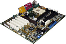
When I first reviewed the Asus A7A266 Socket A motherboard, I quite liked it. Standard Data Rate and Dual Data Rate (SDR and DDR) memory slots, perfectly good built-in sound, decent price.
The first A7A266 I got had a personality defect - one of the sound channels didn't work. I've heard from a couple of other users who've had the same problem, now, which suggests that it wasn't just me. But there's been no great outcry about problems with this board, and when I got a replacement it worked fine. The A7A266 has been around long enough that any ghastly bugs would have been publicised by now; none have arisen. It's a safe purchase. I'm using it in the computer on which I'm writing this.
The A7A266 isn't an exciting motherboard, though.
That's partly because it uses the ALi MAGiK 1 chipset, which performs a few per cent slower than AMD's own 760 chipset and thus offends the sensibilities of those for whom too much speed isn't anything near enough. But the main reason why this board is unexciting is that, out of the box, the A7A266 has lousy overclocking capabilities.
The A7A's BIOS setup program lets you change the CPU's Front Side Bus (FSB) speed, and the processor voltage. This can give you a substantial overclock by itself, if you take a Socket A CPU made for a 100MHz FSB and run it at 133 instead. But there aren't enough FSB options to get the most out of every processor, and FSB overclocking isn't the right way to crank up an Athlon or Duron, anyway. Multiplier overclocking - changing the multiple of the FSB at which the CPU core runs - is. And the A7A266 has no multiplier adjustment feature by default.
This, though, can be changed.
Preparing the processor
To use multiplier adjustment, you need a Socket A CPU with joined L1 bridges.
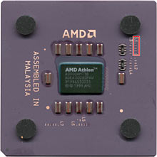
The L1 bridges are four small, but visible to the naked eye, features on top of the chip package, in the location indicated by the little red box in this picture.
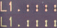
Most, but not all, Socket A chips have their L1 bridges laser-cut when they're assembled. The top half of the above picture shows cut bridges; the bottom half shows uncut ones. If your processor has cut bridges, you have to re-join them with some reasonably conductive substance or other.
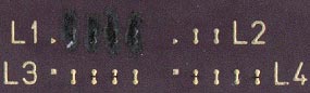
Pencil lead is, famously, perfectly adequate; just put four little pencil lines over the cuts and you're done.
You can also use a circuit board repair pen with conductive ink, if you want a more permanent solution. A few companies sell kits that contain self-adhesive tape patches with tiny conductive stripes to sit on top of the bridges, too.
I felt like getting clever with the AXIA-series Athlon I intended to use on my A7A, though, so I took advantage of the fact that Jaycar Electronics here in Australia had just started stocking conductive varnish, loaded with silver particles and more conductive than pretty much any other room-temperature-solder sort of preparation.
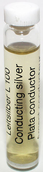
This is what the little varnish vial, Jaycar catalogue number NS3030, price $AU9.95, looks like before you shake it...
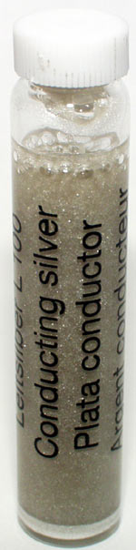
...and this is what it looks like afterwards. There's silver in there, all right.
Unfortunately, I couldn't for the life of me find a way to apply the stuff to a CPU. It wouldn't stick. The CPU surface repelled the liquid, whether I tried to apply it with a pin or with a single fibre from a brush or, I imagine, with a freakin' paint roller. There might have been some surface treatment I could have used to fix the problem, but I didn't know what.
So this varnish may be fabulous for repairing high-current circuit board traces in places where you can't solder, or for impromptu "wiring" in odd places, or indeed for painting your nails, for all I know. But it ain't no good for CPUs. I stuck with the good old pencil.
Incidentally, AMD seem to have an unofficial policy of leaving the L1 bridges uncut on their fastest Athlons. As I write this, that means the 1.33 and 1.4GHz models. It's possible that now that the 1.4GHz Athlon's out, AMD are making 1.33s with cut bridges, and I can't guarantee that every 1.33 is uncut. But I think it's still safe to say that most 1.33s in the market as I write this are the joined-bridge, naturally unlocked type.
If you've got a CPU with factory-joined L1 bridges, no fooling around with pencils or conductive ink is needed. Just plug and go, and if your motherboard supports multiplier adjustment, you can use it.
How do you get it happening on the A7A266, then?
Well, first you update the BIOS.
1004 time
The version 1004 BIOS for the A7A266 adds single-megahertz FSB adjustment and multiplier adjust as well. You can get the BIOS file from Asus here, and then boot from a floppy and use AFLASH.EXE (which you can get from Asus here) to update the BIOS.
If you're not quite so old-school, there's Asus' LiveUpdate Windows updater here that doesn't require the floppy-boot procedure.
When I did my update, LiveUpdate didn't detect the A7A266 yet and so couldn't be used. The current version works.
To activate the software multiplier adjustment, all you have to do is turn on DIP switch 10 on the block of switches down next to the case connector headers, and then...
...what's that you say? You've got an A7A266 with on-board sound, and it doesn't have a DIP switch 10? Just a little block of four switches and some empty solder pads?
Join the club.
Fortunately, the absence of the DIP switches can be overcome.
Little wires
The only DIP switch you need to get software multiplier adjustment happening on the A7A266 is number 10. All of the rest of the missing switches only serve to set CPU configuration when you're not using software-setup mode.
So you don't need to solder on your own DIP switch block, or fly-leads to a bundle of ugly toggle switches. You just need to electrically join the two solder pads, at the end of the pad block, where switch number 10 would go. As motherboard modifications go, this is Baby's First Mobo Hack.
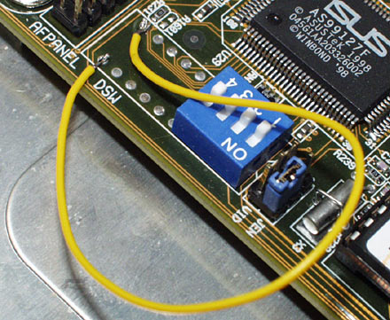
Here's how I did it, with a couple of inches of hook-up wire and a couple of touches from the soldering iron. You could also do it with a line drawn with a conductive-ink pen. I might even have been able to do it with that useless conductive varnish.
I didn't end up using the AXIA CPU on the A7A, because the newer AYHJA-series chips came out. They're the overclockers' darlings of the moment, and are alleged to manage an average overclock above 1.6GHz.
I grabbed a 1.33GHz AYHJA, which was factory unlocked. As AYHJAs go, this one doesn't seem to be terribly exciting; 1533MHz is all it wants to do at less than 1.85 volts, and I don't want to run it at 1.85 with only air cooling (even though I'm using OCZ's excellent Gladiator cooler on it, which got the best score in my CPU cooler comparison here).
But no matter. Both the 1MHz-increment FSB adjustment...
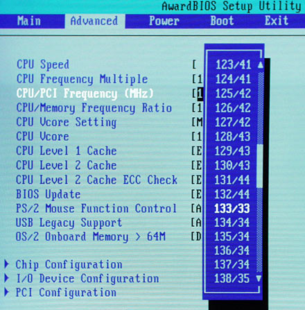
...and the multiplier adjustment...
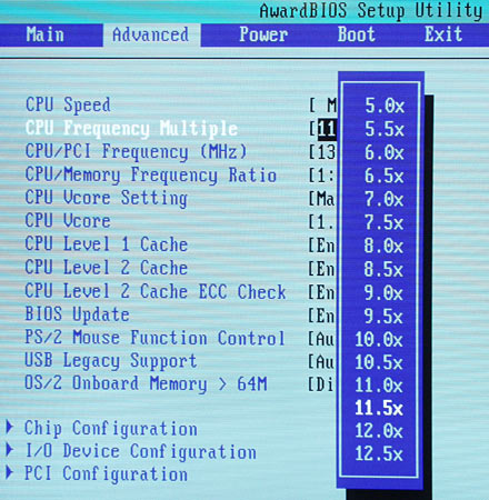
...work fine. The multiplier setup's mildly odd - current Athlons interpret the "12.5X" setting as "13X" - but that's not a serious problem.
FSB adjustment's not actually very useful if you've already got multiplier adjustment. It just lets you eke out that last percentage point or two, which if you ask me is better left untouched. If you don't wind your CPU up absolutely as far as it can go, you've got more crash-avoidance leeway. And the difference between, 1533MHz and, say, 1560MHz (which is a perfectly plausible ceiling speed for a CPU that won't do 1600), is only 1.7%. You are not going to notice that.
Overall
If you've never modified a motherboard, hacking an A7A266 is a good beginner project. With a conductive pen, you wouldn't even need to solder anything.
Some motherboard hacks are amazingly involved - yards and yards of ultra-fine wire applied over multiple evenings by Japanese enthusiasts apparently attempting to turn their motherboard into a time machine.
This is not one of those hacks.
Thanks to this hack, and the strategic application of an AYHJA Athlon, I now have a processor which scores 4670 MIPS and 1915 MFLOPS in a meaningless CPU-twiddling benchmark.
In 1988, my Amiga 500 did 0.7 MIPS.
Heh heh heh.
What about the A7M?
Asus' AMD-chipset cousin to the A7A266, the A7M266, is another board that's missing DIP switches needed for multiplier adjustment. It can be fixed, too, but it's a more complex operation.
This page on Overclockers Australia will show you how.